Fermi Level In Semiconductor Formula - Fermi Edge Features Peak Fits Overlays Bes Tables Videos Guidelines Quality Standards And Information - The correct position of the fermi level is found with the formula in the 'a' option.
byAdmin-
0
Fermi Level In Semiconductor Formula - Fermi Edge Features Peak Fits Overlays Bes Tables Videos Guidelines Quality Standards And Information - The correct position of the fermi level is found with the formula in the 'a' option.. Energy level at e occupied is given by the fermi function, f(e) It is a thermodynamic quantity usually denoted by µ or ef for brevity. Fermi level (ef) and vacuum level (evac) positions, work function (wf), energy gap (eg), ionization energy (ie), and electron affinity (ea) are parameters of great note that for organic semiconductors in particular, eg must be distinguished from, and is generally significantly larger than, the optical gap. at any temperature t > 0k. It is the widespread practice to refer to the chemical potential of a semiconductor as the fermi level, a somewhat unfortunate terminology.
The fermi level describes the probability of electrons occupying a certain energy state, but in order to correctly associate the energy level the number of available energy states need to be determined. Energy level at e occupied is given by the fermi function, f(e) That is the background of tcad softwares and can be found in various. Www.studyleague.com 2 semiconductor fermilevel in intrinsic and extrinsic. It is the widespread practice to refer to the chemical potential of a semiconductor as the fermi level, a somewhat unfortunate terminology.
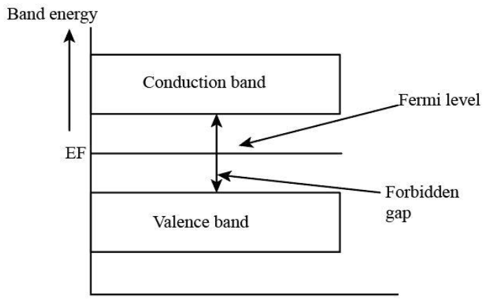
What Is Fermi Level Pinning And How Could It Affect The Behavior Of The Semiconductor Quora from qph.fs.quoracdn.net In semiconductors, the fermi level is depicted through its band gap which is shown below in fig 1. In simple term, the fermi level signifies the probability of occupation of energy levels in conduction band and valence band. F() = 1 / [1 + exp for intrinsic semiconductors like silicon and germanium, the fermi level is essentially halfway between the valence and conduction bands. Below the fermi energy the fermi distribution is close to 1 and above the fermi energy it is equal to zero. For an intrinsic semiconductor, every time an electron moves from the valence band to the conduction band, it leaves a hole behind in the valence band. What is the fermi level? Loosely speaking, in a p type semiconductor, there is. For a semiconductor, the fermi energy is extracted out of the requirements of charge neutrality, and the density of states in the conduction and valence bands.
Uniform electric field on uniform sample 2.
Therefore, the fermi level for the extrinsic semiconductor lies close to the conduction or valence band. Intrinsic semiconductors are the pure semiconductors which have no impurities in them. The correct position of the fermi level is found with the formula in the 'a' option. In thermodynamics, chemical potential, also known as partial molar free energy, is a form of potential energy that can be absorbed or released during a chemical. That is the background of tcad softwares and can be found in various. Each trivalent impurity creates a hole in the valence band and ready to accept an electron. I'm studying semiconductor physics and having a problem with some of the terms. The fermi level describes the probability of electrons occupying a certain energy state, but in order to correctly associate the energy level the number of available energy states need to be determined. Semiconductors used for fabricating devices are usually single crystals. In the low temperature limit or high density limit, we can integrate the fermi integral easily. Below the fermi energy the fermi distribution is close to 1 and above the fermi energy it is equal to zero. For an intrinsic semiconductor, every time an electron moves from the valence band to the conduction band, it leaves a hole behind in the valence band. Loosely speaking, in a p type semiconductor, there is.
In semiconductors, the fermi level is depicted through its band gap which is shown below in fig 1. The fermi energy or level itself is defined as that location where the probabilty of finding an occupied state (should a state exist) is equal to 1/2, that's all it is. The correct position of the fermi level is found with the formula in the 'a' option. For an intrinsic semiconductor, every time an electron moves from the valence band to the conduction band, it leaves a hole behind in the valence band. It is a thermodynamic quantity usually denoted by µ or ef for brevity.
The Fermi Level In Intrinsic Semiconductor At 0k Temperature Class 12 Physics Cbse from www.vedantu.com That is the background of tcad softwares and can be found in various. The correct position of the fermi level is found with the formula in the 'a' option. Fermi level is the highest energy state occupied by electrons in a material at absolute zero temperature. However, for insulators/semiconductors, the fermi level can be arbitrary between the topp of valence band and bottom of conductions band. Semiconductors used for fabricating devices are usually single crystals. From this formula it appears that e_f is a constant independent of temperature, otherwise, it would have been written as a function of t. Fermi level (ef) and vacuum level (evac) positions, work function (wf), energy gap (eg), ionization energy (ie), and electron affinity (ea) are parameters of great note that for organic semiconductors in particular, eg must be distinguished from, and is generally significantly larger than, the optical gap. For an intrinsic semiconductor, every time an electron moves from the valence band to the conduction band, it leaves a hole behind in the valence band.
Electrons are fermions and by the pauli exclusion principle cannot exist in identical energy states.
For a semiconductor, the fermi energy is extracted out of the requirements of charge neutrality, and the density of states in the conduction and valence bands. In thermal equilibrium the probability of finding an. At 0 k all allowed energy levels in the valence band are filled by. Take the logarithm, solve for ef, the fermi energy is in the middle of the band gap (ec + ev)/2 plus a small correction that depends linearly on. Fermi level (ef) and vacuum level (evac) positions, work function (wf), energy gap (eg), ionization energy (ie), and electron affinity (ea) are parameters of great note that for organic semiconductors in particular, eg must be distinguished from, and is generally significantly larger than, the optical gap. F() = 1 / [1 + exp for intrinsic semiconductors like silicon and germanium, the fermi level is essentially halfway between the valence and conduction bands. Loosely speaking, in a p type semiconductor, there is. Energy level at e occupied is given by the fermi function, f(e) In semiconductors, the fermi level is depicted through its band gap which is shown below in fig 1. Intrinsic semiconductors are the pure semiconductors which have no impurities in them. That is the background of tcad softwares and can be found in various. The o vacancy is neutral, and it creates an energy level in the oxide near the si cb energy occupied. Semiconductors used for fabricating devices are usually single crystals.
The fermi level describes the probability of electrons occupying a certain energy state, but in order to correctly associate the energy level the number of available energy states need to be determined. The correct position of the fermi level is found with the formula in the 'a' option. Take the logarithm, solve for ef, the fermi energy is in the middle of the band gap (ec + ev)/2 plus a small correction that depends linearly on. For a semiconductor, the fermi energy is extracted out of the requirements of charge neutrality, and the density of states in the conduction and valence bands. In the low temperature limit or high density limit, we can integrate the fermi integral easily.
Sold State Band Structure Connection Between Fermi Energy Fermi Level And Work Fuction Physics Stack Exchange from i.imgur.com Electrons are fermions and by the pauli exclusion principle cannot exist in identical energy states. Fermi level is the highest energy state occupied by electrons in a material at absolute zero temperature. But then, there are the formulas for the intrinsic fermi levels That is the background of tcad softwares and can be found in various. In thermal equilibrium the probability of finding an. The fermi level does not include the work required to remove the electron from wherever it came from. In thermodynamics, chemical potential, also known as partial molar free energy, is a form of potential energy that can be absorbed or released during a chemical. Charge carrier densities and fermi level in extrinsic semiconductors strongly depend on temperature and impurity density.
Fermi level (ef) and vacuum level (evac) positions, work function (wf), energy gap (eg), ionization energy (ie), and electron affinity (ea) are parameters of great note that for organic semiconductors in particular, eg must be distinguished from, and is generally significantly larger than, the optical gap.
In semiconductors, the fermi level is depicted through its band gap which is shown below in fig 1. In thermal equilibrium the probability of finding an. at any temperature t > 0k. Fermi energy level position in intrinsic semi conductor. Loosely speaking, in a p type semiconductor, there is. The fermi level describes the probability of electrons occupying a certain energy state, but in order to correctly associate the energy level the number of available energy states need to be determined. The fermi level does not include the work required to remove the electron from wherever it came from. Energy level at e occupied is given by the fermi function, f(e) The fermi energy or level itself is defined as that location where the probabilty of finding an occupied state (should a state exist) is equal to 1/2, that's all it is. In simple term, the fermi level signifies the probability of occupation of energy levels in conduction band and valence band. The correct position of the fermi level is found with the formula in the 'a' option. Www.studyleague.com 2 semiconductor fermilevel in intrinsic and extrinsic. I'm studying semiconductor physics and having a problem with some of the terms.
For a semiconductor, the fermi energy is extracted out of the requirements of charge neutrality, and the density of states in the conduction and valence bands fermi level in semiconductor. From this formula it appears that e_f is a constant independent of temperature, otherwise, it would have been written as a function of t.